CDZ3.6B
Diodes
1/4
Zener diode
CDZ3.6B
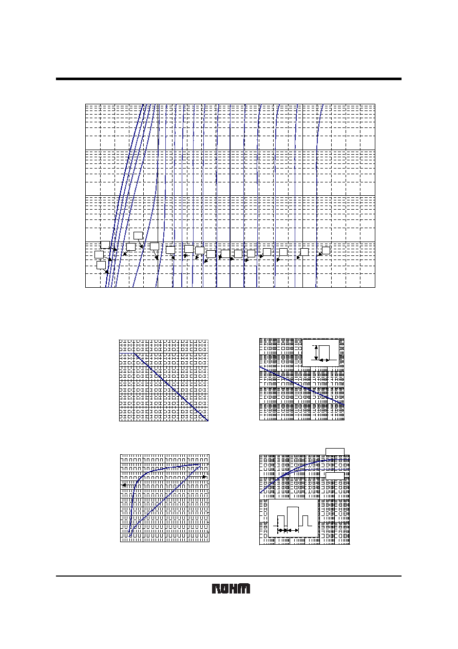
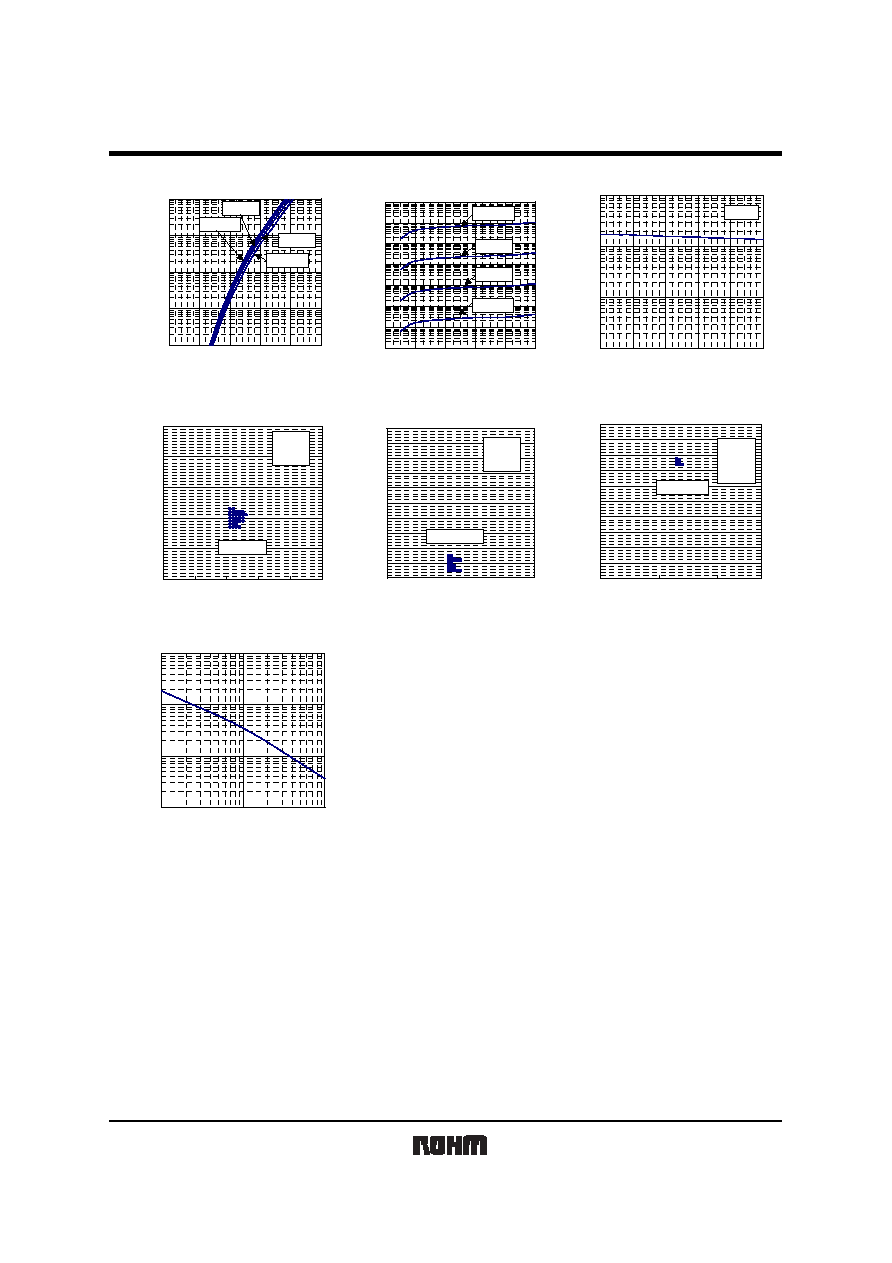
Applications
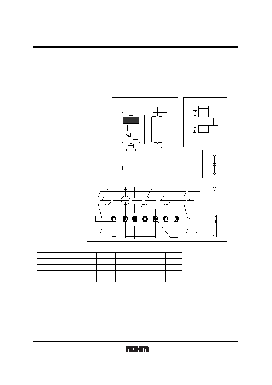
External dimensions (Unit : mm) Land size figure (Unit : mm)
Constant voltage control
Features
1) 2-pin ultra mini-mold type for high-density
mounting (VMN2).
2) High reliability.
3) Can be mounted automatically, using chip
mounter.
Structure
ROHM : VMN2
EX. CDZ3.6B
dot (year week factory) + day
0.16±0.05
0.37±0.03
0.6±0.05
0.35±0.1
0.
9±
0.
05
1.
0±
0.
05
0.156
VMN2
0.55
0.
5
0.
45
0.
45
Construction
Silicon epitaxial planar
Taping specifications (Unit : mm)
0.7±0.05
4.0±0.1
2±0.05
0.5
4±0.1
2±0.05
1.55
1.
7
5
±
0
.
1
8.
0±
0.
2
3.
5±
0.
05
1.
1±
0.
05
0.2±0.05
0.52
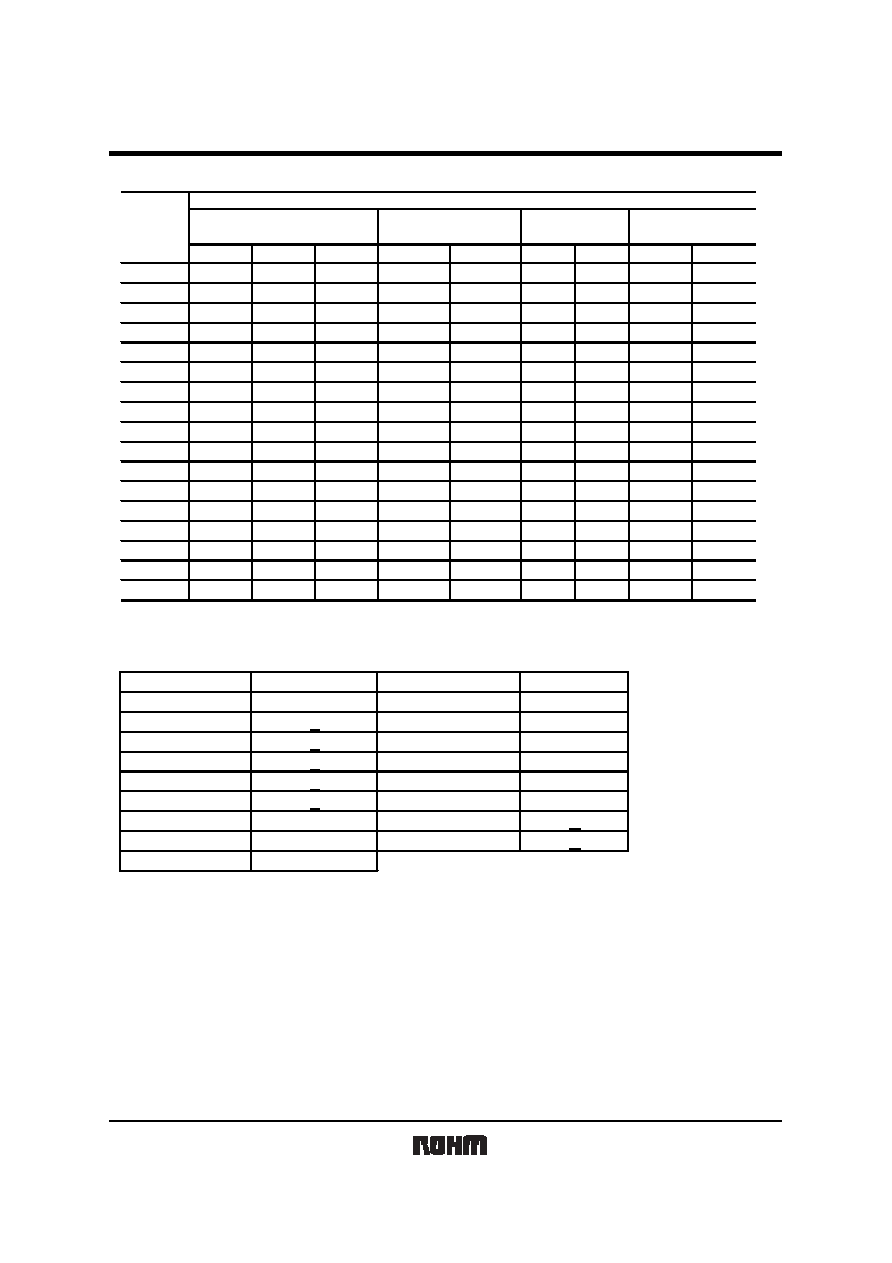
Absolute maximum ratings (Ta=25
°
C)
Symbol
Unit
P
m
Tj
Tstg
Topr
Operating temperature
-55 to +150
Parameter
Junction temperature
Storage temperature
Power dissipation
Limits
150
-55 to +150
100
W
Appendix
Appendix1-Rev1.1
The products listed in this document are designed to be used with ordinary electronic equipment or devices
(such as audio visual equipment, office-automation equipment, communications devices, electrical
appliances and electronic toys).
Should you intend to use these products with equipment or devices which require an extremely high level of
reliability and the malfunction of with would directly endanger human life (such as medical instruments,
transportation equipment, aerospace machinery, nuclear-reactor controllers, fuel controllers and other
safety devices), please be sure to consult with our sales representative in advance.
Notes
No technical content pages of this document may be reproduced in any form or transmitted by any
means without prior permission of ROHM CO.,LTD.
The contents described herein are subject to change without notice. The specifications for the
product described in this document are for reference only. Upon actual use, therefore, please request
that specifications to be separately delivered.
Application circuit diagrams and circuit constants contained herein are shown as examples of standard
use and operation. Please pay careful attention to the peripheral conditions when designing circuits
and deciding upon circuit constants in the set.
Any data, including, but not limited to application circuit diagrams information, described herein
are intended only as illustrations of such devices and not as the specifications for such devices. ROHM
CO.,LTD. disclaims any warranty that any use of such devices shall be free from infringement of any
third party's intellectual property rights or other proprietary rights, and further, assumes no liability of
whatsoever nature in the event of any such infringement, or arising from or connected with or related
to the use of such devices.
Upon the sale of any such devices, other than for buyer's right to use such devices itself, resell or
otherwise dispose of the same, no express or implied right or license to practice or commercially
exploit any intellectual property rights or other proprietary rights owned or controlled by
ROHM CO., LTD. is granted to any such buyer.
Products listed in this document are no antiradiation design.
About Export Control Order in Japan
Products described herein are the objects of controlled goods in Annex 1 (Item 16) of Export Trade Control
Order in Japan.
In case of export from Japan, please confirm if it applies to "objective" criteria or an "informed" (by MITI clause)
on the basis of "catch all controls for Non-Proliferation of Weapons of Mass Destruction.